


2026-02-10
Semiconductor and Advanced Packaging Solutions
-
Home >> Application >> Semiconductor
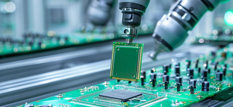
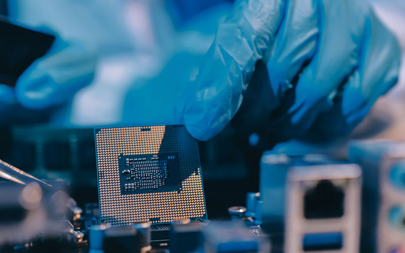
For high-value-added, high-technical-barrier packaging and testing processes, we provide highly reliable precision machining capabilities.
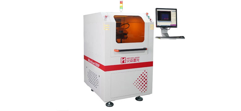
Packaging Substrate Processing Solutions: For brittle substrates such as ceramics and glass, ceramic laser cutters and UV picosecond laser cutters enable high-purity, low-thermal-stress precision cutting and marking.
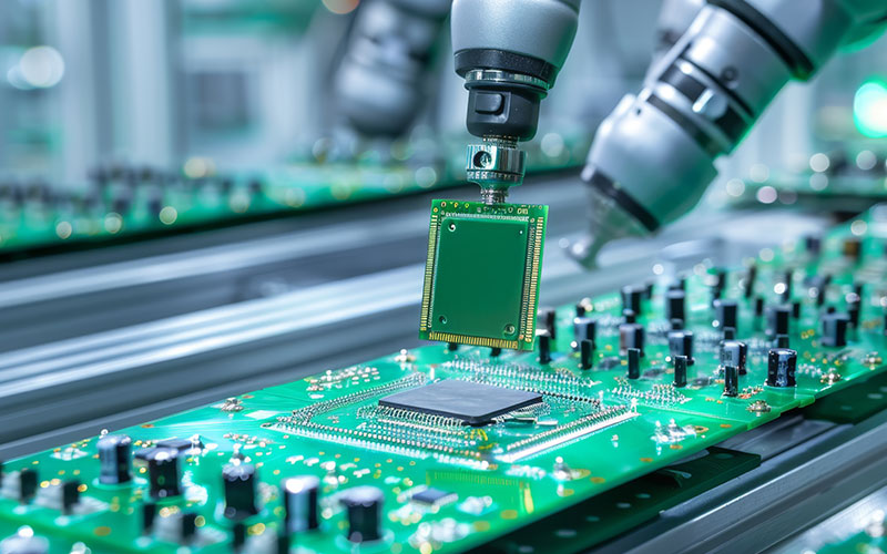
Advanced Packaging Micro-machining Solutions: In cutting-edge packaging technologies such as Fan-Out and Wafer-Level Chip Scale Packaging (WLCSP), picosecond/femtosecond lasers are employed for critical processes including wafer bonderless dicing, Through-Silicon Via (TSV) formation, and micro-bump trimming, with virtually no thermal damage.


Access the latest industry solutions and case studies
Contact us by telephone or email to resolve your concerns.


