


2020-07-10
Applications of Ultraviolet Lasers in High-End Precision Machining
-
Home >> News >> Industry Trends
I. Core Advantages (Why Choose Ultraviolet Lasers?)
High Photon Energy: Ultraviolet light possesses short wavelengths (commonly 355nm, extending to 266nm in deep ultraviolet), with individual photons delivering high energy. This enables direct disruption of chemical bonds in most materials (photochemical effect), rather than merely melting them through thermal effects.
"Cold Processing" Effect: Upon absorbing UV laser energy, materials transition directly from solid to gas (sublimation) or plasma states. This minimises the heat-affected zone, virtually eliminating slag formation, micro-cracks, and thermal stress deformation. This is pivotal for achieving "precision" machining.
Small Diffraction Limit: According to optical diffraction principles, the diameter of a laser's focused spot is proportional to its wavelength. The short wavelength of ultraviolet light enables focusing to extremely small spots (sub-micrometre scale), facilitating ultra-fine processing.
High Absorption by a Wide Range of Materials: Most metals, polymers, ceramics, glass, sapphire, and similar materials exhibit significantly higher absorption rates for ultraviolet light than for infrared or visible light, resulting in high processing efficiency.
II. Primary Application Fields
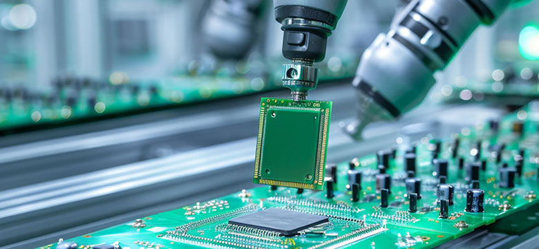
1. Semiconductor and Microelectronics Manufacturing
This represents the most advanced and demanding application domain for ultraviolet lasers.
Wafer Dicing: Used to cut brittle wafers such as silicon, silicon carbide, gallium arsenide, and sapphire. The cold processing characteristics of UV lasers prevent chipping and stress introduced by traditional dicing wheels, enhancing chip yield and strength.
PCB/FPC Precision Processing:
HDI Board Drilling: Drilling minute through-holes and blind holes for interlayer interconnections.
FPC Cutting and Window Opening: Precision cutting of flexible circuit boards to remove cover layers without damaging underlying conductors.
Chip Marking and Traceability: Creating permanent, clear, stress-free micron-level markings (e.g., QR codes, serial numbers) on chip surfaces without compromising chip structure.
Stripping and Repair: Removing specific coatings and repairing defects in thin-film transistor arrays.
2. Precision Medical Devices and Biotechnology
Cardiovascular Stent Cutting: Single-pass precision cutting of complex stent structures from tubular materials such as nickel-titanium alloys and stainless steel. Cuts are smooth and burr-free, eliminating the need for post-processing and significantly enhancing stent fatigue life and biocompatibility.
Medical Catheter Punching: Creation of precision micro-hole arrays on polymeric catheters.
Surgical Instrument Marking: Permanent marking compliant with medical device UDI (Unique Device Identification) regulations.
Microfluidic Chip Fabrication: Processing micrometre-scale channels and reaction chambers on glass or polymer substrates.
3. New Materials and Brittle Material Processing
Glass/Sapphire Cutting and Punching: Custom cutting and micro-perforation for mobile phone camera lenses, smartwatch covers, and optical components, delivering smooth edges and high strength.
Ceramic Substrate Cutting and Scoring: For applications including LED and power device packaging.
Polymer Film Precision Processing: Such as cutting polyimide films for OLED displays and scoring PET solar backsheets.
4. Precision Marking and Surface Treatment
White/Dark Marking: Achieving high-contrast, non-damaging markings through chemical reactions that induce colour changes on certain plastics (e.g., ABS).
Surface microtexturing: Fabricating micrometre-scale regular patterns on material surfaces (e.g., hydrophobic/hydrophilic surfaces, adhesion-enhanced surfaces, optical diffraction structures).
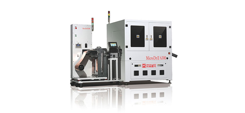
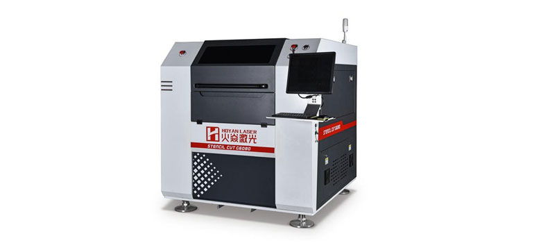
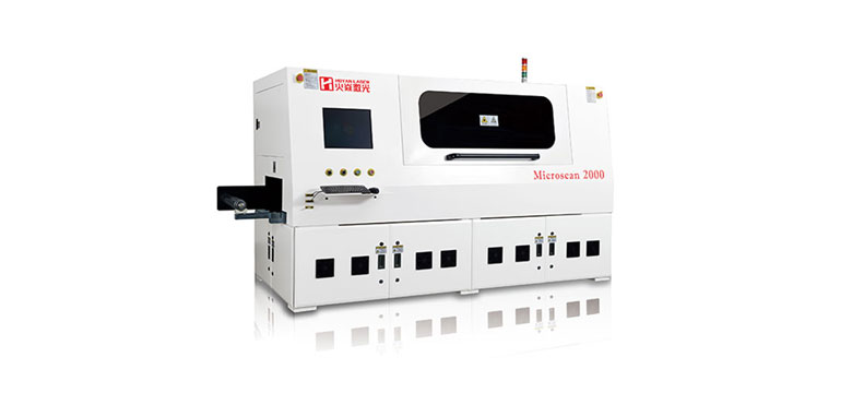
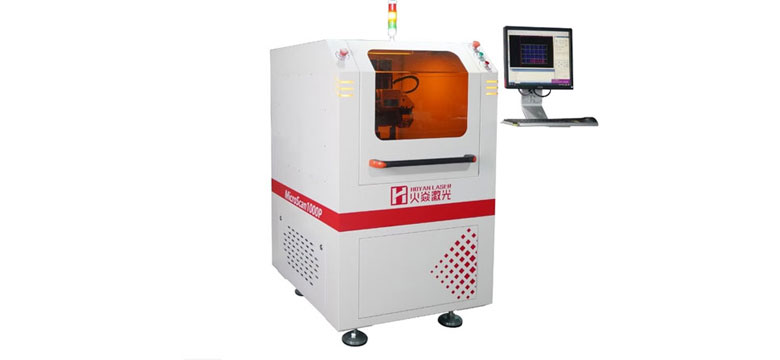
5. Specialised Applications for Equipment in Your Images
Combined with your provided equipment list, these represent direct applications of UV lasers:
UV laser drilling machines: Primarily used for micro-hole drilling in high-end PCBs/IC substrates, achieving apertures as small as 20-30 micrometres.
SMT Laser Stencil Cutter: Utilises UV lasers to cut openings in stainless steel or nickel plates for SMT stencil templates, delivering exceptional precision with smooth hole walls that directly influence solder paste printing quality.
FPC/PCB UV Laser Cutter: Performs contour precision cutting, slotting, and windowing on flexible and rigid circuit boards without mechanical stress, yielding clean edges.


Access the latest industry solutions and case studies
Contact us by telephone or email to resolve your concerns.


